
SEM-EDS Analysis
Our SEM-EDS analysis services provide high-resolution imaging and elemental characterization to support a wide range of metallurgical and materials evaluations. From investigating the root cause of component failures to examining microstructure, coatings, and powders, SEM-EDS gives precise, reliable insights that help ensure quality, performance, and compliance with industry standards.
We offer specialized services including fracture analysis to identify crack initiation and failure mechanisms, plating and coating thickness measurements for uniformity and durability, and metallographic analysis to characterize microstructure and phases. Our high magnification inspections reveal wear patterns, microcracks, and material transfer, while failure analysis provides actionable insights to prevent future issues. Additionally, we perform particle morphology and powder imaging to evaluate size, shape, distribution, and composition, supporting additive manufacturing, coatings, and advanced materials applications. By combining state-of-the-art SEM imaging with elemental analysis, our team helps industries optimize processes, validate materials, and ensure long-term reliability.
Request a Quote for SEM-EDS Analysis
Imaging Capabilities
- Fracture analysis (Fractography)
Fracture analysis using SEM-EDS allows detailed examination of failed components to identify the root cause of cracks, fractures, or catastrophic failures. High-resolution imaging reveals fracture surfaces, crack initiation sites, and microstructural features, while elemental analysis identifies contaminants or inclusions that may have contributed to failure. This service is critical for industries like aerospace, automotive, and energy to prevent future failures and improve component design and reliability.
- Plating thickness
Using SEM-EDS, we can accurately measure plating and coating thickness at the micro and nanoscale, providing detailed insight into layer uniformity and potential defects. This non-destructive evaluation ensures that coatings meet design specifications, enhance corrosion resistance, and maintain long-term component performance.
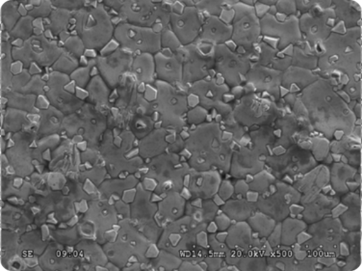
- Metallographic analysis
SEM-EDS metallographic analysis provides high-magnification imaging and elemental mapping to characterize microstructure, phase distribution, and inclusions. This analysis supports quality control, process optimization, and material verification across a wide range of metals, alloys, and advanced materials.
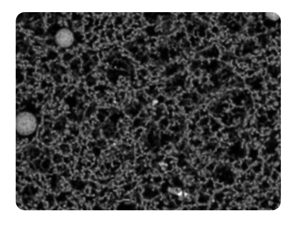
- Particle Morphology
Through particle morphology analysis, SEM-EDS reveals particle size, shape, and composition, providing essential data for powders, slurries, and composite materials. This information is crucial for optimizing performance, quality, and consistency in additive manufacturing, coatings, and other industrial processes.
- Failure Analysis
SEM-EDS failure analysis combines microstructural imaging with elemental characterization to investigate component failures in detail. By identifying the source of defects, corrosion, or fracture mechanisms, we provide actionable insights that guide design improvements and prevent recurring issues.
- High magnification inspection – wear patterns, microcracks, material transfer
Our high magnification SEM-EDS inspections detect subtle surface defects such as wear patterns, microcracks, and material transfer. This level of analysis helps clients predict component lifespan, validate manufacturing processes, and ensure reliability in high-stress applications.
-
Powder Imaging
Powder imaging using SEM-EDS delivers high-resolution images and elemental analysis of metal, ceramic, and polymer powders. This evaluation allows precise characterization of particle distribution, morphology, and composition, supporting quality control, process development, and material certification for critical applications in additive manufacturing, 3D printing and cold spray
Determination Of Chemical Composition:
- Parent alloy
- Residues & stains
- Foreign object debris
- Powders
- Surface contaminants
- Inclusion determination
- Alloy segregation
- EDS features include Micro Probing, X-Ray Mapping, and Line Scanning
Quality Accreditations


ISO/NADCAP/GE/PW Accredited
Certified to deliver precise, internationally recognized results.
Fast Turnaround Times
Quick, efficient processing to keep your manufacturing timelines on track.
Experience Matters
Our team of seasoned engineers and techs bring decades of hands-on industry knowledge.
Detailed & Defensible Reports
Clear, illustrated reports with actionable insights and data integrity.
Why choose us?
Trusted by leading industry professionals for reliable result, expert analysis and unmatched quality of service.
About SMS Labs
Sturbridge Metallurgical Services was founded in 1990 in Sturbridge, MA, by President, Courtney Grimes. Our small, independent testing lab has outgrown three locations through the years, before settling into our current home at 8 Picker Road in Sturbridge, Massachusetts. Our lab offers a complete range of materials testing and analysis services, and we've expanded into sales of a full line of metallographic equipment and supplies.
Learn more